- 您现在的位置:买卖IC网 > Sheet目录2008 > MAX1400CAI+ (Maxim Integrated Products)IC ADC 18BIT LP 28-SSOP
MAX1400
+5V, 18-Bit, Low-Power, Multichannel,
Oversampling (Sigma-Delta) ADC
_______________________________________________________________________________________
7
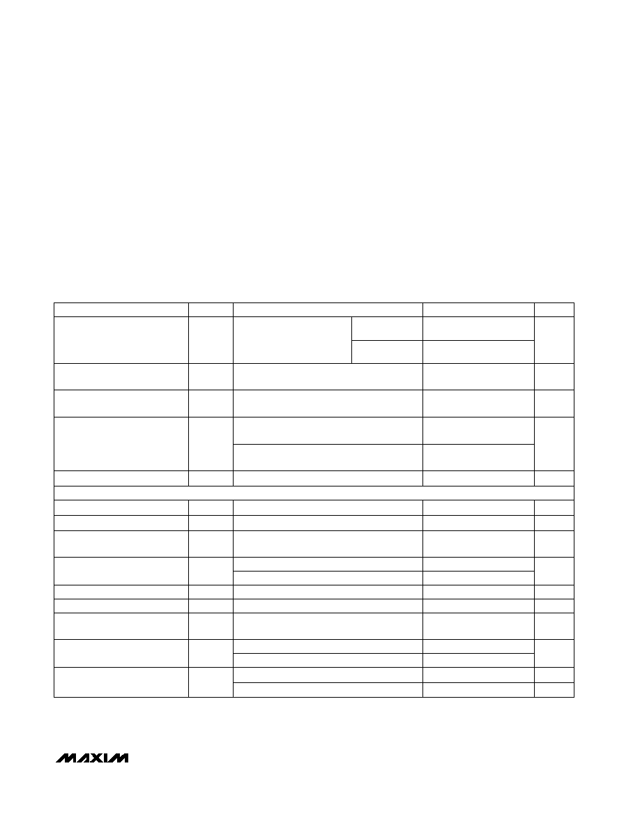
Note 16: Measured at DC in the selected passband. PSR at 50Hz will exceed 120dB with filter notches of 25Hz or 50Hz and FAST
bit = 0. PSR at 60Hz exceeds 120dB with filter notches of 20Hz or 60Hz and FAST bit = 0.
Note 17: PSR depends on gain. For a gain of +1V/V, PSR is 70dB typical. For a gain of +2V/V, PSR is 75dB typical. For a gain of
+4V/V, PSR is 80dB typical. For gains of +8V/V to +128V/V, PSR is 85dB typical.
Note 18: Standby power-dissipation and current specifications are valid only with CLKIN driven by an external clock and with the
external clock stopped. If the clock continues to run in standby mode, the power dissipation will be considerably higher.
When used with a resonator or crystal between CLKIN and CLKOUT, the actual power dissipation and IDD in standby
mode depends on the resonator or crystal type.
TIMING CHARACTERISTICS
(V+ = +5V ±5%, VDD = +2.7V to +5.25V, AGND = DGND, fCLKIN = 2.4576MHz; input logic 0 = 0V; logic 1 = VDD, TA = TMIN to TMAX,
unless otherwise noted.) (Notes 19, 20, 21)
0100
VDD = 3.3V
VDD = 5V
VDD = 3.3V
VDD = 5V
Bus Relinquish Time After SCLK
Rising Edge (Note 26)
t10
10
100
ns
SCLK Falling Edge to Data Valid
Delay (Notes 24, 25)
t6
080
ns
INT High Time
tINT
560 / N
x tCLKIN
ns
X2CLK = 1, N = 2(2 x MF1 + MF0)
X2CLK = 1
X2CLK = 0
SCLK Setup to Falling Edge CS
t4
30
ns
SCLK Low Pulse Width
t8
100
ns
10
70
100
ns
VDD = 5V
CS Rising Edge to SCLK Rising
Edge Hold Time
t9
0
ns
(Note 21)
SCLK High Pulse Width
t7
100
ns
CS Falling Edge to SCLK Falling
Edge Setup Time
t5
30
ns
280 / N
xtCLKIN
INT to CS Setup Time
t3
X2CLK = 0, N = 2(2 x MF1 + MF0)
0
ns
(Note 8)
RESET Pulse Width Low
t2
100
ns
Master Clock Input Low Time
fCLKIN LO
0.4 x
tCLKIN
ns
tCLKIN = 1 / fCLKIN, X2CLK = 0
Master Clock Input High Time
fCLKIN HI
0.4 x
tCLKIN
ns
tCLKIN = 1 / fCLKIN, X2CLK = 0
Master Clock Frequency
fCLKIN
0.8
5.0
MHz
Crystal oscillator or clock
externally supplied for
specified performance
(Notes 22, 23)
PARAMETER
SYMBOL
MIN
TYP
MAX
UNITS
0.4
2.5
CONDITIONS
SCLK Rising Edge to INT High
(Note 27)
t11
200
ns
VDD = 3.3V
SERIAL-INTERFACE READ OPERATION
发布紧急采购,3分钟左右您将得到回复。
相关PDF资料
MAX1401CAI+
IC ADC 18BIT LP 28-SSOP
MAX1415AEWE+T
IC ADC 16BIT DELTA SIGMA 16-SOIC
MAX1421CCM+D
IC ADC 12BIT 40MSPS 48LQFP
MAX1426EAI+T
IC ADC 10BITS 10MSPS 28SSOP
MAX1434ECQ+D
IC ADC 10BIT 50MSPS 100-TQFP
MAX1444EHJ+T
IC ADC 10BIT 40MSPS 32-TQFP
MAX1499ECJ+
IC ADC 3 1/2DIG W/LED DVR 32TQFP
MAX152EPP+
IC ADC 8BIT 1UA PWR-DWN 20-DIP
相关代理商/技术参数
MAX1400CAI+T
功能描述:模数转换器 - ADC 18-Bit 5Ch 4.8ksps 2.5V Precision ADC RoHS:否 制造商:Texas Instruments 通道数量:2 结构:Sigma-Delta 转换速率:125 SPs to 8 KSPs 分辨率:24 bit 输入类型:Differential 信噪比:107 dB 接口类型:SPI 工作电源电压:1.7 V to 3.6 V, 2.7 V to 5.25 V 最大工作温度:+ 85 C 安装风格:SMD/SMT 封装 / 箱体:VQFN-32
MAX1400CAI+W
制造商:Maxim Integrated Products 功能描述:
MAX1400CAI-T
功能描述:模数转换器 - ADC RoHS:否 制造商:Texas Instruments 通道数量:2 结构:Sigma-Delta 转换速率:125 SPs to 8 KSPs 分辨率:24 bit 输入类型:Differential 信噪比:107 dB 接口类型:SPI 工作电源电压:1.7 V to 3.6 V, 2.7 V to 5.25 V 最大工作温度:+ 85 C 安装风格:SMD/SMT 封装 / 箱体:VQFN-32
MAX1400EAI
功能描述:模数转换器 - ADC RoHS:否 制造商:Texas Instruments 通道数量:2 结构:Sigma-Delta 转换速率:125 SPs to 8 KSPs 分辨率:24 bit 输入类型:Differential 信噪比:107 dB 接口类型:SPI 工作电源电压:1.7 V to 3.6 V, 2.7 V to 5.25 V 最大工作温度:+ 85 C 安装风格:SMD/SMT 封装 / 箱体:VQFN-32
MAX1400EAI+
功能描述:模数转换器 - ADC 18-Bit 5Ch 4.8ksps 2.5V Precision ADC RoHS:否 制造商:Texas Instruments 通道数量:2 结构:Sigma-Delta 转换速率:125 SPs to 8 KSPs 分辨率:24 bit 输入类型:Differential 信噪比:107 dB 接口类型:SPI 工作电源电压:1.7 V to 3.6 V, 2.7 V to 5.25 V 最大工作温度:+ 85 C 安装风格:SMD/SMT 封装 / 箱体:VQFN-32
MAX1400EAI+T
功能描述:模数转换器 - ADC 18-Bit 5Ch 4.8ksps 2.5V Precision ADC RoHS:否 制造商:Texas Instruments 通道数量:2 结构:Sigma-Delta 转换速率:125 SPs to 8 KSPs 分辨率:24 bit 输入类型:Differential 信噪比:107 dB 接口类型:SPI 工作电源电压:1.7 V to 3.6 V, 2.7 V to 5.25 V 最大工作温度:+ 85 C 安装风格:SMD/SMT 封装 / 箱体:VQFN-32
MAX1400EAI-T
功能描述:模数转换器 - ADC RoHS:否 制造商:Texas Instruments 通道数量:2 结构:Sigma-Delta 转换速率:125 SPs to 8 KSPs 分辨率:24 bit 输入类型:Differential 信噪比:107 dB 接口类型:SPI 工作电源电压:1.7 V to 3.6 V, 2.7 V to 5.25 V 最大工作温度:+ 85 C 安装风格:SMD/SMT 封装 / 箱体:VQFN-32
MAX1400EVKIT
制造商:Maxim Integrated Products 功能描述:MAX1402 EVALUATION KIT/EVALUATION SYSTEM - Boxed Product (Development Kits)